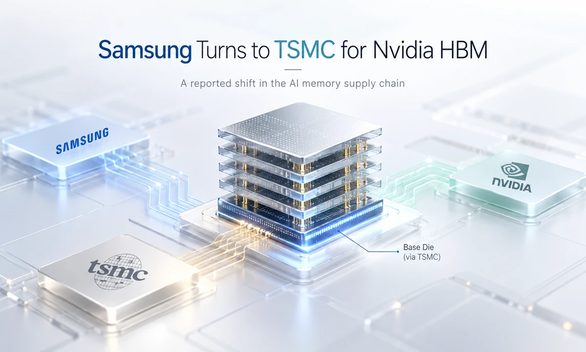
Samsung Electronics will have rival foundry TSMC manufacture a key component of the custom memory it is developing for Nvidia, a notable shift away from Samsung's all-in-house approach, though none of the three companies has publicly confirmed it.
Samsung Electronics will use Taiwan's TSMC, the world's largest contract chipmaker to produce the “base die” for Nvidia's next-generation custom high-bandwidth memory (HBM), the Seoul Economic Daily reported on Sunday, 18 October 2026, citing unnamed industry sources. The Reuters news agency and several technology outlets carried the report the same day. As of 19 October 2026, Samsung, TSMC and Nvidia have not issued any official statement confirming the arrangement, so it should be treated as a report rather than a done deal.
What the report actually claims
To understand the news, it helps to know how an HBM chip is built. HBM is a tall stack of memory layers used alongside AI accelerator chips (GPUs). The stack has two parts: the “core dies,” which are the actual DRAM memory layers, and a single “base die” at the bottom, which acts as the logic layer that connects the memory to the processor.
Until now, Samsung has made both parts itself, the memory and the logic base die, a self-contained model the industry calls “turnkey.” According to the Seoul Economic Daily, Samsung has decided to break from that model for one specific product and let TSMC build the base die using its advanced 3-nanometre (3nm) process.
The report says the request came from Nvidia. Nvidia has reportedly asked all three of its memory suppliers, Samsung, SK Hynix and Micron to make the base die for this custom memory on TSMC's 3nm process, and to standardise the memory (core) dies on a sixth-generation DRAM process known internally as “1c.”
The catch: Samsung is handing a strategic step to its biggest rival
The significant angle here is competitive, not technical. TSMC and Samsung are direct rivals in the foundry (contract chip manufacturing) business. Earlier in 2026, Samsung's distinguishing pitch for this exact project was that it could do everything in-house, unlike SK Hynix and Micron, which already rely on TSMC for their advanced base dies. If the report is accurate, Samsung is now giving up that in-house edge for Nvidia's custom memory and routing the work to its fiercest competitor.
The reported reason is yield, the share of chips that come out of a production line usable rather than defective. The Seoul Economic Daily put TSMC's 3nm yield above 90%, versus around 60% for Samsung Foundry's comparable 2nm (SF2) process. For a product where consistency across suppliers matters, Nvidia appears to be prioritising a proven, high-yield process.
There are important limits to the shift, and they are easy to miss:
It is selective. Samsung reportedly plans to keep its in-house turnkey model for standard HBM products, and for custom HBM it supplies to other customers such as AMD. The TSMC arrangement is specific to Nvidia's custom memory.
Samsung is hedging. The report says Samsung is still testing whether it could make this base die at its own foundry too — a fallback in case Nvidia's demand outstrips TSMC's available capacity. In other words, the plan is not described as exclusive or final.
It is unconfirmed. Every detail traces back to the Seoul Economic Daily's industry sources. No company has confirmed it on the record.
What this custom memory is, and why Nvidia wants it
Nvidia unveiled the custom memory, reported as “NVHBM,” in August 2026. The key idea is that Nvidia moves its own memory controller, the circuitry that manages how data flows in and out of memory, out of the GPU and into the HBM base die itself. Doing this standardises how the memory behaves regardless of which company manufactured it, and reduces the work of validating each supplier's product separately.
According to the Seoul Economic Daily, this redesign is based on the architecture of HBM4E (the seventh-generation HBM). The report says relocating the controller shrinks the base die's physical interface area by about 60% compared with standard HBM, which it says can widen bandwidth by up to 30% and cut power use by roughly 15% versus standard HBM4E. These figures come from the newspaper's reporting, not from official Nvidia specifications, and should be read as reported estimates.
How this fits Nvidia's roadmap
This is not Samsung's first HBM win with Nvidia. Samsung has reported mass-producing its current sixth-generation HBM4 earlier in 2026 using its own in-house 4nm base die for Nvidia's Vera Rubin platform. Nvidia has said its Rubin GPU generation is targeted for commercial release in the second half of 2026. The custom NVHBM, based on HBM4E, is widely reported to be aimed at Nvidia's later Rubin-series accelerators expected in 2027.
The move also reflects a broader industry trend. SK Hynix shifted its HBM4 base-die production to TSMC's logic process earlier, and if this report holds, all three major memory makers would be leaning on TSMC for their most advanced base dies, strengthening TSMC's position across the AI hardware supply chain.
Why it matters beyond Korea
HBM is the memory that feeds the AI GPUs powering data centres worldwide including the cloud and AI infrastructure that Indian enterprises, startups and cloud providers increasingly depend on. Anything that affects the yield, cost or supply of this memory can ripple through to the availability and price of AI computing globally.
That supply backdrop is tight. Investment bank UBS, cited in the Seoul Economic Daily's reporting, forecasts HBM demand next year at roughly 61.5 billion gigabits up about 91% from this year against expected shipments of around 54.6 billion gigabits, implying a shortfall of about 10%. In that context, Samsung's reported decision to prioritise a high-yield, high-capacity partner like TSMC while keeping its own foundry on standby reads as a response to an expected crunch.
What buyers and industry watchers should keep in mind
This is a business-to-business component story, not a consumer product launch. There is no retail product, launch date, or price attached to it in Korea, India or anywhere else, so any specific pricing claim you may see elsewhere about these memory chips should be treated with caution unless a company confirms it.
The practical takeaways: the report signals how fiercely Nvidia is standardising its memory supply chain, how much leverage TSMC now holds, and the pressure on Samsung's foundry business to close a yield gap with its rival. Whether Samsung ultimately uses TSMC, its own foundry, or both for this memory remains to be seen.
What is known, and what is still uncertain
What is reported
- Samsung will reportedly use TSMC's 3nm process for the base die of Nvidia's custom NVHBM.
- Nvidia has reportedly asked Samsung, SK Hynix and Micron to standardise on TSMC's 3nm base die and a sixth-generation (1c) DRAM core die.
- Samsung is said to be keeping its in-house model for standard HBM and for other customers, and is testing its own foundry as a backup.
What remains unconfirmed:
- No official confirmation from Samsung, TSMC or Nvidia.
- Final volumes, timing, contract terms and whether the arrangement is exclusive.
- The exact performance figures, which so far come from media reporting rather than official specifications.

With experience writing 500+ pieces of content across different formats, I focus on making technology and cybersecurity topics clear, informative, and accessible. At **TechJox**, I cover tech news, cybersecurity trends, digital safety, and practical guides that help readers stay informed and make better decisions. My approach combines research, accuracy, and simple storytelling to turn complex information into useful, engaging, and easy-to-understand content.
Discussion (0)
You need a free TechJox account to join the discussion and report scams you spot.